Thursday, February 29, 2024

Semiconductor Materials for Flexible and Transparent Electronics

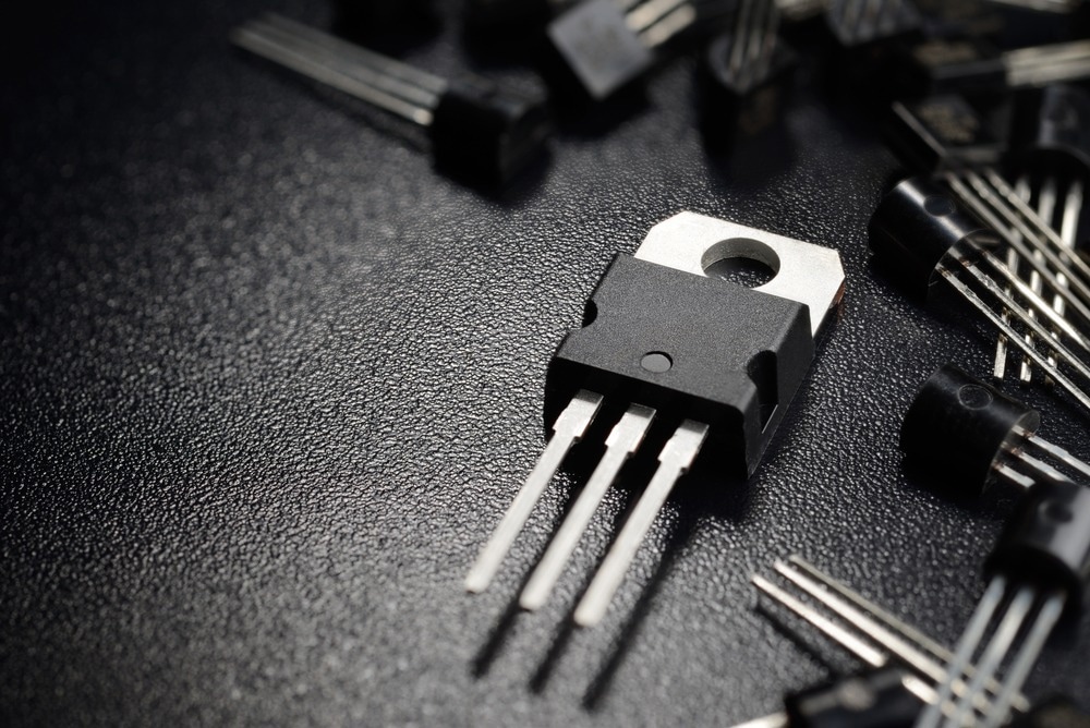
 Semiconducting materials are the primary building blocks for electronic devices. As new coating techniques influence the development of flexible and transparent electronics, researchers look to semiconductor materials to innovate these devices further.

Semiconductor Materials for Flexible and Transparent Electronics

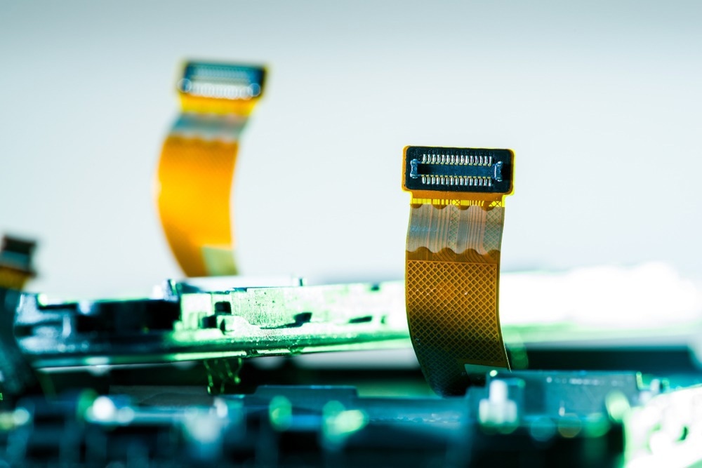
Image Credit: P A/Shutterstock.com

Flexible and Transparent Electronics: Current Market

A market survey for transparent electronics reported by IDTechEx predicts market growth of twenty billion dollars by 2041. According to the report, thin film transistors (TFTs), display devices, photovoltaics, smart windows are a few of the transparent electronics likely to be the highest in demand.

Another report by IDTechEX showcases the importance of flexible electronics and predicts the roadmap of such technologies. Various applications such as flexible displays, textile electronics, electronic skin patches need semiconductors that cover large areas over the flexible substrates.

Many multinational companies are involved in the flexible and transparent electronics industry. For example, KODAK reportedly offers a state-of-the-art facility for the fabrication of flexible and transparent devices to researchers for the manufacture of prototypes.

Samsung Electronics Co. Ltd., LG Electronics, 3M Co., E Ink Holding Inc. are other examples of flexible and transparent electronics manufacturers.

Semiconductors for Flexible and Transparent Electronics

Generally speaking, the materials mainly studied for transparent and flexible electronics are amorphous semiconductors, semiconducting transparent oxides, metal chalcogenides, and nanowires.

A journal article published in Advanced Materials by Sun et al. summarizes work exploring the application of inorganic semiconducting materials as a coating for plastic substrates.

Amorphous silicon (a-Si) is one of the dominant materials in semiconductor industry after the single crystalline Si. As for flexible devices, single-crystal Si is not suitable for flexible electronics because of its brittle nature. Hence, a-Si is preferred over single-crystal silicon for various applications.

Amorphous semiconductors are more commonly used for flexible devices due to the possibility of large-scale uniform deposition of these materials having low-temperature processibility.

One publication in Nature demonstrated the fabrication of transparent thin film transistors (TFT) using transparent amorphous oxide semiconductors (amorphous-In-Ga-Zn-O, referred as, a-IGZO). High charge mobility, room temperature processing and stable performance under bending conditions were found to be the material's advantages.

2D Semiconductors for Flexible and Transparent Electronics

Semiconducting transition metal dichalcogenides (TMDs) have attracted much attention from researchers due to their structural behavior. These materials are reported to have a layered structure, with properties relating to the number of layers. Such tunability of their properties makes it a favorable material for flexible and transparent electronics.

Two-dimensional materials are the most suitable materials for flexible and transparent electronics. Heterostructures of such 2D materials are reported to have excellent flexibility, transparency and charge transport properties. Other 2D semiconducting materials reported include transition metal oxides and metal chalcogenides.

In work published by Das et al., demonstrated the fabrication of transparent TFT composed of entirely 2D materials. The TFTs had a monolayer of graphene as the metal electrodes, hexagonal boron nitride (h-BN) as a dielectric material and tungsten diselenide (WSe2) as a semiconducting material.

The carrier mobility in the transistor was recorded ~100 times more than that recorded by a-Si-based TFTs. The device showed good temperature stability, along with several other parameters ideal for enhancing TFTs.

In another work by Yu et al., large-scale deposition of two-dimensional graphene and molybdenum disulfide (MoS2) heterostructure was achieved through chemical vapor deposition. The work reports of high-performing devices and circuits fabricated with the heterostructure, the performances of which were compared with the traditional MoS2-metal contact.

Future Scope and Commercial Viability

Much research is towards the direction of developing alternate materials and coating techniques with the goal of decreasing the device cost and increasing the performance.

Various substrates are explored that can be applied to blendable and stretchable electronics. Substrates such as metallic foils, plastic sheets and paper were explored as substrates for flexible devices.

Building devices over flexible and transparent substrates have few constraints, such as processing temperature. Plastic substrates are much more suitable for such applications but require a processing temperature below the glass transition temperature, after which the plastic will degrade.

Research interest in this area extends to devices that could have the properties of stretchability. Developing such devices is reported to be possible by employing elastomeric substrates with strong molecular interactions.

Investigations into flexible and transparent materials and substrates for device fabrication could open up a wide range of exciting applications such as flexible lighting, wearable charging devices, implantable bioelectronics, wearable sensors that could monitor the health of patients, novel display architecture for consumer electronics and many more.

Flexible and transparent electronics have a long way to go before being available for consumer use. With increased interest in the applications of semiconductor materials in this field, we are likely to see the field grow in the future.


Reference and Further Reading

IDTechEx. Available at: https://www.idtechex.com/en/research-report/transparent-electronics-materials-markets-2021-2041/795.

Tuesday, February 27, 2024

New Transistors for Ground-Breaking Semiconductors

A limiting problem in creating energy-efficient circuits for improved memory and more powerful computers is manufacturing a transistor with reconfigurable properties. As the size of transistors becomes smaller and the need for higher data processing capabilities increases, it becomes clear that more innovative solutions are required to overcome these obstacles. A potential solution is having reconfigurable transistors made up of ferroelectrics which can change their properties even after manufacturing, allowing for flexible and efficient circuits. 

New Transistors for Semiconductors, reconfigurable transistors, ferroelectric transistors

Image Credit: Andrei Kuzmik/Shutterstock.com

Tapping into the Power of Transistors

Transistors are small electrical components that, while having simple functions of letting current pass or stopping it, accomplish very complex tasks. The speed of rapidly turning on or off gives way to the processing speed in computers. These transistors are the foundations upon which modern digital technology is built.

As the technology moves forward, these transistors keep getting smaller, essentially accomplishing almost twice the performance in the same area. Roughly, this is known as Moore’s law, which dictates that, with time, smaller transistors can be placed on a board, thus increasing processing capabilities. However, as the size of transistors approaches the nanoscale, quantum mechanical effects such as leakage current and tunneling effect come into play, and electrons start behaving in ways that do not remain very predictable.

Cutting-edge semiconductor materials such as ferroelectrics play a role in this context. These remarkable substances possess an attribute called "ferroelectricity," enabling them to alter their polarization when subjected to an external electric field.

The incorporation of ferroelectrics in transistor design has the potential to bring about a shift by introducing a state beyond the conventional "On" and "Off" states. This novel characteristic introduces the concept of a state enabling enhanced data storage and processing capabilities, ultimately resulting in efficient and adaptable transistors, as well as the birth of neuromorphic circuits for mimicking human-brain synapses in a computer.

Ferroelectrics to the Rescue

Researchers at Lund University have recently shown how new reconfigurable transistors can be made using these astounding ferroelectrics. Using a blend of materials, scientists have developed ferroelectric "grains" that regulate an electrical tunnel junction within the transistor.


These grains are incredibly tiny, measuring 10 nanometers in size. By analyzing variations in voltage or current, they have successfully detected shifts in polarization within each grain, providing insights into how these changes impact the behavior of the transistor.

The remarkable aspect of the findings lies in the ability to generate tunnel junctions by utilizing grains positioned right next to the junction. These tiny grains can now be individually manipulated, whereas before, only collective groups of grains called ensembles could be monitored.

This breakthrough allows for the identification and control of portions within the material. Additionally, the researchers have explored how this understanding can be applied to create reconfigurable applications by manipulating the signal that passes through the transistor in ways.

Enter Ferroelectric Tunnel Field-effect Transistors (Ferro-TFET)

Picture this - reconfigurability, a smaller footprint, and reduced supply voltage, all harmoniously working together to deliver a signal modulation spectacle like never before. A symphony of efficiency and versatility, all in a single transistor.

Recently, in a captivating exposition, researchers embarked on a journey to unveil the groundbreaking capabilities of a single vertical nanowire ferroelectric tunnel field-effect transistor (ferro-TFET). This remarkable creation published in Nature Communications not only boasts the ability to modulate input signals but also showcases a mesmerizing array of diverse modes, including signal transmission, phase shift, frequency doubling, and seamless mixing with a conspicuous suppression of undesired harmonics - a true marvel tailor-made for reconfigurable analog applications.

At the core of this awe-inspiring breakthrough lies a novel heterostructure design, a feat of ingenuity that places a gate and source in the delightful overlap. The result? A nearly perfect parabolic transfer characteristic, charmingly adorned with robust negative transconductance.

Furthermore, a ferroelectric gate oxide introduces a non-volatile reconfigurability to this ferro-TFET, thus, resulting in a stunning ensemble of high-density, energy-efficient, and multifunctional digital/analog hybrid circuits.

Single Domain Dynamics & Defects – An Achilles Heel to Scaled Ferroelectrics

Diving into the realm of cutting-edge technology, the quest for ultra-scaled ferroelectrics emerges as the holy grail for high-density nonvolatile memories and next-gen neuromorphic computing. But, here's the catch - to tackle advanced applications, we must unravel the enigmatic mysteries of single-domain dynamics and the elusive behavior of defects, all within those scaled ferroelectrics.

One such study was published in Applied Sciences and Engineering, which ventured into the groundbreaking integration of a ferroelectric gate stack onto a heterostructure tunnel field-effect transistor (TFET) boasting sub-thermionic operation. Without physical gate-length scaling required for conventional transistors, the localized potential variations induced by single domains and individual defects were sensed based on the ultrashort effective channel created by the band-to-band tunneling process.

It was shown by the scientists that ferroelectric films could be integrated into heterostructure devices and that the opportunity for ultrasensitive scale-free detection of single domains and defects in ultra-scaled ferroelectrics was provided by the intrinsic electrostatic control within ferroelectric TFETs.

This pioneering approach opens up vast opportunities for ultrasensitive detection within ultra-scaled ferroelectrics, driving us closer to the dream of high-density nonvolatile memories and cutting-edge neuromorphic computing.

The Pursuit of Progress

The enigmatic fusion of ferroelectric semiconductors and reconfigurable transistors embarks us on a journey into uncharted territory within digital electronics. As we traverse this unexplored frontier, the promise of energy-efficient transistors endowed with extraordinary adaptability becomes the clarion call of a transformative era on the horizon.

However, while the trajectory of progress unfurls with tantalizing possibilities, the road ahead remains shrouded in intriguing complexity and challenges that demand our unwavering dedication and optimism.

More from AZoM: Alternative Electrode Materials for High-Performance Batteries

References and Further Reading

ScienceDaily, (2023). Cutting-edge transistors for semiconductors of the future. [Online]
Available at: https://www.sciencedaily.com/releases/2023/07/230703133015.htm


Monday, February 26, 2024

Topological insulators could herald a new future for electronics


Experimental studies of elementary particles and atoms as well as the application of quantum mechanics to describe their behavior have revolutionized our understanding of the structure of matter and led to unprecedented rates of technical progress in the 20th century.

Even the smallest of differences between how various types of atoms and molecules interact can lead to vastly different properties in bulk materials. For example, one material might conduct electrical current while another acts as an insulator or even superconductor — all related to how electrons are allowed to move and interact within them.

Recently, scientists have begun to study more exotic materials, those whose surfaces behave differently from the properties of the overall bulk material. One of the most interesting of these are known as topological insulators.

“Topological insulators are novel materials that allow [electricity conduction without heat loss] along the edges but remain insulating in the bulk,” explained Xiaoling Wang, professor at the University of Wollongong, Australia, in an email. “Such edge state conduction is associated with quantum mechanical properties unique to the bulk state of topological insulators, and differentiates topological insulators from ordinary insulators, which are insulating in the bulk as well as along the edges.”

These materials are very promising for applications in future electronics. However, their usefulness could be enhanced if the electrons running along their surfaces share the same polarization — this refers to the direction of their internal rotation, also referred to as their “spin”.

This would lead to the application of topological insulators in spintronics, a field of electronics whose operation depends on the spins of current carriers with the potential to bring about more efficient computer memory, hard drives, quantum computers, and much more.

Searching for the right material

To find such materials, Wang and his colleague Muhammad Nadeem at the University of Wollongong studied the interaction of electrons in two-dimensional (2D) (that is, one atom thick) ribbons of different materials.

“The significance of 2D materials is multifold,” Nadeem explained, outlining of the rationale behind their research direction. “On the one hand, 2D materials host unique physical properties [that are] tunable via extrinsic stimuli [such as electric field, strain, or illumination]. On the other hand, they promise energy-efficient and miniaturized devices for information and communication technologies due to exotic quantum mechanical functionalities and reduced dimensionalities.”

In their study published in Advanced Physics Research, the physicists analyzed antiferromagnets — materials in which atomic spins align in a regular pattern with neighboring spins having opposite directions. Topological insulators based on these materials are of particular interest since antiferromagnets are minimally influenced by an external magnetic field,  safeguarding electronics built using these materials against outside perturbations.

To study these materials, the team used a well-established model that describes the interaction of electrons in solids. They found that 2D antiferromagnetic ribbons turn into topological insulators with polarized electrons at their boundary edge — an interface or perimeter where the material transitions from one state to another, often exhibiting distinct properties or behaviors — but only under very specific conditions.

“This work predicts the existence and practical realization of a new class of topological quantum material called topological Dirac spin-gapless materials.‎ These materials host unique chiral edge states,” Wang said. “In other words, all the edge states carry the same spin-polarization, a key feature for devising spintronic technologies.”

The physical behavior they predict is not specific to one particular material, which opens up many possibilities for future practical applications in industry and science.

“The proposed mechanisms are material-independent and can be employed for emergent spintronic devices, such as graphene spintronics,” explained Nadeem.

Although this theoretical result is exciting, there is still a lot of work to be done to put it into practice and build real spintronic devices based on the materials they predicted.

“This work needs further attention on two fronts,” concluded Nadeem. “First, modeling and simulation for energy efficiency and performance of quantum devices based [topological insulators with polarized electrons at the boundary edge], and second, finding suitable materials which host robust spin-gapless chiral edge states and are integrable with current spintronic technologies.”

Reference: Muhammad Nadeem and Xiaolin Wang, Topological Dirac Spin-Gapless Materials — a New Horizon for Topological Spintronics Without Spin-Orbit Interaction, Advanced Physics Research (2023). DOI: 10.1002/apxr.202300028

Monday, February 19, 2024

Embedded system module targets the AI IPC market


DFI is targeting the AI application market by launching the MTH968 embedded system module (SOM) equipped with the latest Intel® Core™ Ultra processor.

t is the first product integrated with an NPU (Neural Processor Unit) processor, representing the official integration of AI with industrial PCs (IPCs). With the expansion into AI IPC, DFI expects to inject new momentum into the AI edge computing market.

According to the STL Partners report, the potential market value of global edge computing will increase from US$9 billion in 2020 to US$462 billion in 2030, representing a compound annual growth rate (CAGR) of 49%. Therefore, the development of products that utilize the core capabilities of chips to rapidly execute AI edge computing in devices has become a key focus for many major technology companies.

The MTH968 adopts the COM Express (COM.0 R3.1) Type 6 module standard and is equipped with an Intel Meteor Lake processor, marking the debut of integrated CPU, GPU, and NPU on a single chip. Two “low-power, high-efficiency cores (LP E-core)” are built in, reducing power consumption by 30% to 50%, optimizing the CPU by 10%, and improving GPU performance by up to 114% compared to previous generation Intel processors.

The built-in NPU of Meteor Lake enhances the performance of the MTH968 in critical AI tasks. Based on a new artificial intelligence computing architecture, the device can more efficiently process advanced AI edge computing, complex graphics computing, and other applications, while saving data on cloud costs.

The MTH968 has highly customizable integration capabilities and a fanless wide temperature design(operating from -40°C to 85°C), and utilizes DDR5 and NVMe SSD to optimize high-efficiency computing performance, reduce latency, and enhance storage speed. The MTH968 can be widely used in AIoT fields such as industrial automation, smart transportation, and smart agriculture.

As 5G, edge computing, and remote control tech advance, IPCs directly handle complex tasks through AI edge computing. The MTH968 excels in high-performance computing with account energy efficiency, enhancing computing and customizable flexibility, thereby accelerating industrial AI application upgrades.

https://electronicmaterialsconference.com/

Thursday, February 15, 2024

Exploring the Dynamic Growth of Multilayer Printed Circuit Boards: Market Trends and Insights


Multilayer printed circuit boards (PCBs) are witnessing a surge in demand, fueled by the rapid advancement in electronic devices across various industries.

Multilayer printed circuit boards (PCBs) play a pivotal role in modern electronic devices and systems, serving as a crucial platform for interconnecting electronic components and facilitating signal and power flow. These PCBs are comprised of multiple layers of copper traces and insulating substrate materials bonded together, enabling higher circuit density, improved signal integrity, and greater functionality compared to single or double-layer PCBs.

The global multilayer PCB market is experiencing consistent growth, driven by increasing demand for electronic devices, technological advancements, and the expanding array of applications necessitating complex and compact circuitry.

In 2021, the market size of Multilayer Printed Circuit Boards (PCBs) amounted to USD 78.9 billion. Projections indicate a steady rise from USD 82.36 billion in 2022 to USD 128.5 billion by 2030, with a compound annual growth rate (CAGR) of 5.68% during the forecast period (2023-2030).

Multilayer Printed Circuit Boards are gaining traction owing to their myriad technical advantages, including compact size, lightweight construction, high quality, enhanced durability, improved flexibility, and the ability to establish more potent single connection points. The demand for compact and lightweight solutions in smartphones and computers is effectively met through the utilization of multilayer printed circuit boards.

Download a sample copy of Report:
www.marketdigits.com/request/sample/600 

Multilayer Printed Circuit Board Market Top Player’s Company Profiles

Key Points:

Enquiry :
www.marketdigits.com/request/enquiry/600

Key Trends:

Recent Industry News:

Monday, February 12, 2024

Materials Discovery to Enable Computers that Think More Like Humans


Artificial intelligence is already transforming how we work and live, automating time-consuming tasks and streamlining our decision-making.

However, AI algorithms are mostly run on conventional complementary metal oxide semiconductor (CMOS)-based hardware. This requires them to be trained with large datasets to accomplish even the simplest tasks, such as image analysis or facial recognition. Processing these data-intensive requests requires vast computing resources, like data centers. The process consumes significant amounts of energy.

A USC Viterbi School of Engineering research team has discovered a new semiconductor with a unique material property that can enable more energy-efficient computing hardware that functions like the human brain. Two related research papers were published recently in the journals Advanced Materials and Advanced Electronic Materials. The research is led by Huandong Chen, a 2023 Materials Science Ph.D. graduate in the Mork Family Department of Chemical Engineering and Materials Science, from the group of Jayakanth Ravichandran, an associate professor in chemical engineering and materials science and electrical and computer engineering.

The human brain is excellent at associative learning — we have an innate ability to call up memories, make connections, and understand objects and stimuli in relation to each other. Human brains utilize interconnected neurons and synapses to store information locally where it is processed. Our brains are capable of handling highly sophisticated tasks and operating at remarkably low energy consumption. Developing neuromorphic computing hardware — hardware that mimics the architecture and operation of the human brain — is highly desired in the quest to achieve energy-efficient advanced computing.

Hardware materials that mimic the brain

If a material can move abruptly between two states (also known as phase transitions), this provides the foundation for hardware that mimics the brain. For example, a slight difference in temperature dramatically changes a material’s electrical conductivity — the ease of passing an electrical current — from a high to a low value, or vice versa. Such neuron-inspired phase change devices have been achieved only in a handful of materials.

The USC Viterbi researchers discovered novel electronic phase transitions in a semiconductor and leveraged those intriguing physical properties to demonstrate an abrupt electrical conductivity change with varying temperature and applied voltage, which can enable the development of energy-efficient neuromorphic computing.

Ravichandran holds the Philip and Cayley MacDonald Endowed Early Career Chair. His group has been working on a semiconductor material known as barium titanium sulfide (BaTiS3) since 2017. The group’s work resulted in the BaTiS3 material showing a world-record high birefringence property — a phenomenon in which a ray of light is split into two rays. In a recent unrelated work, they discovered an even higher value in a related material.

“However, as a semiconductor, we do not expect any abrupt phase transition in BaTiS3,” said Ravichandran.

“Naively thinking, this material should behave like a ‘boring’ semiconductor without any expectation of a phase transition,” said Chen.

A surprising discovery

Ravichandran and his group were surprised to observe the signatures of phase transitions in the BaTiS3 material when measuring its electrical properties under different temperatures. Upon cooling the material, the electrical resistivity of BaTiS3 increases, and it undergoes a transition at around 240 Kelvin (about -33° Celsius), featuring an abrupt change in electrical conductivity. With further cooling, it continues to increase until 150 Kelvin (about -123° Celsius), after which the material goes through another transition with increased electrical conductivity.

“It is always exciting to observe abnormal behavior in our experiments, but we have to check carefully to make sure that those phenomena are real and reproducible,” said Ravichandran.

In this work, Chen performed careful experiments to rule out contributions from many extrinsic factors, such as contact resistance and strain status, which could complicate this effect. It was demonstrated that the unique property originated within the material itself.

“This is particularly important when characterizing such a new material system. One good example of not ruling out other factors was the recent drama surrounding the so-called room temperature superconductor LK-99, where it seems the sharp drop in resistivity at around 105° Celsius is likely from an impurity, known as Cu2S”, said Chen.

The team also investigated how the crystal structure of the BaTiS3 material changes during these electronic phase transitions, corresponding to the changes in electrical conductivity.

Boyang Zhao, a Materials Science Ph.D. candidate from Ravichandran’s group, traveled to the synchrotron at Lawrence Berkeley National Lab to map out the structure evolution. By combining the information from the electrical and structural measurements — which are key experimental features for the interesting phenomena called charge density wave phase transition — the team could claim the existence of charge density wave order in BaTiS3.

“We’ve discovered one very special charge density wave phase change material. Most charge density wave materials only go from a metal state — which is high conductivity to an insulator state — which is low conductivity. What we have found is that you can go from a low conductivity state to a low conductivity state. Such insulating-to-insulating transition is very, very rare, with only a handful of examples out there. So, scientifically, it’s very interesting,” said Ravichandran.

How the phase transitions in BaTiS3 work is not fully understood yet. The team collaborated with Rohan Mishra’s group from Washington University in St. Louis, performing materials modeling to obtain a deeper understanding of the material system. Current experimental and theoretical findings suggest that the observed phase change phenomena have an unexpected origin compared to most charge density wave materials. The team is conducting further studies to understand this phenomenon better.

The latest Advanced Materials research on novel phase change material discovery was conducted with collaborators from the University of Washington in Seattle, Washington University in St. Louis, Columbia University, Oak Ridge National Laboratory, and Lawrence Berkley National Laboratory.

A prototype showing the material in action

In a follow-up work that was recently published in Advanced Electronic Materials, Chen and his collaborators fabricated the first prototype neuronal device using the BaTiS3 material. They were able to show abrupt switching by varying current and voltage. They also showed oscillations in voltage that signified fast switching between two states in the phase transition. Similar voltage oscillations are observed in the brain.

“This is an important step towards actual electronic device applications of BaTiS3. It is also quite exciting to see such a short period of time between this prototype device demonstration and the fundamental material property discovery,” said Chen.

The frequency of voltage oscillations was altered by the operation temperature and channel sizes. A lower operation temperature and a shorter device channel size give rise to higher oscillation frequencies.

“We expect that much more sophisticated neuronal functionalities can be achieved by connecting multiple BaTiS3 neurons to each other or integrating with other passive synaptic devices, as has been successfully demonstrated in another phase change system VO2. Future efforts in making this material in the thin film form that features phase transitions and is potentially compatible with our semiconductor manufacturing could be of great interest to both the research community and the semiconductor industry,” said Chen.

This work in Advanced Electronic Materials was done in collaboration with Robert G. and Mary G. Lane Endowed Early Career Chair Han Wang’s group in USC’s Ming Hsieh Department of Electrical and Computer Engineering. Other authors include Materials Science Ph.D. candidate Nan Wang and Electrical Engineering Ph.D. candidate Hefei Liu.

Ravichandran serves as a co-director for the Core Center of Excellence in NanoImaging (CNI).

Ravichandran and his research team at USC are supported by the MURI program of the Army Research Office and the U.S. National Science Foundation’s Ceramics Program.

Chiral Powers Next-Generation Electronics With Nanomaterials as It Raises $3.8m

  Chipmaking has become one of the world’s most critical technologies in the last two decades. The main driver of this explosive growth has ...