Saturday, April 13, 2024

Chiral Powers Next-Generation Electronics With Nanomaterials as It Raises $3.8m

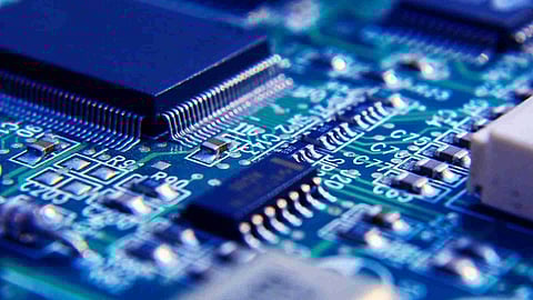
 Chipmaking has become one of the world’s most critical technologies in the last two decades. The main driver of this explosive growth has been the continuous scaling of silicon technology (widely known as the Moore’s Law).


But these advances in silicon technology are slowing down, as we reach the physical limits of silicon. For this reason, the industry has been investing heavily in nanomaterials like carbon nanotube, graphene and TMDs, which are expected to enable chips with unprecedented functionality. However, making electronic devices with these extremely small materials at speed, with precision, and without compromising on quality has been a long-standing obstacle.

Nanotechnology company Chiral is today announcing a $3.8m funding round to address this challenge head on, innovating the way nanomaterials are integrated into devices. Its expertise in nanotechnology, automation, and high-precision robotics will be pivotal in the industry’s move beyond silicon to the next generation of electronics. The pre-seed funding round was co-led by Founderful (formerly Wingman Ventures) and HCVC and includes grants from ETH Zurich and Venture Kick.

Research has evidenced the use case and impact of nanomaterials across a range of electronics including high-performance transistors, low-power sensors, quantum devices, and many more. However, existing production methods, mostly based on chemistry, are not controllable, which has thus far prevented commercialization of these devices.

Chiral has built high-speed, automated, robotic machines that integrate nanomaterials into devices. These machines can robotically place micrometer-sized (or even nanometer-sized) materials on small chips. Repeating these motions in a fast and automated manner requires a very high level of engineering, which, when done right, ensures the precision and control that conventional chemistry-based methods lack.

The development of Chiral’s technology started as a national research project conducted at the Swiss Federal Institutes of Technology (ETH Zurich, EPFL, and Empa), in which the company’s co-founders, Seoho Jung, Natanael Lanz, and Andre Butzerin participated as PhD students. After 4 years of R&D, the research team finished its first prototype machine, which was 100 times faster than the other systems available at the time. The immediate reaction of the market to the prototype, which quickly led to the company’s first batch of pilot customers, convinced the co-founders that they should continue their activity as a company. They incorporated Chiral in June 2023 as a result.

Seoho Jung, Co-founder and CEO at Chiral commented: “At Chiral, we are pioneering the next generation of electronic devices across industry. Chipmakers are aware of the potential of nanomaterials and we’re bringing that potential to life. This funding will accelerate the development of our next machine, which will unlock new market opportunities with its versatility and performance. We are also excited to scale our team to keep up with the growing demand and customer base."

The global nanotechnology market size is projected to grow from $79.14 billion in 2023 to $248.56 billion by 2030, at a CAGR of 17.8% (Fortune business insights research). One of the largest chipmakers in the world, Taiwan Semiconductor Manufacturing Company (TSMC) presented its development roadmap showing nanomaterial-based transistors as its future architecture. 

Pascal Mathis, Founding Partner at Founderful, commented: “We're thrilled to join forces with Chiral alongside HCVC. Chiral's AI- and robotics-based technology lets us envision a future where nanomaterial-based chips are being produced at the scale needed for commercialization – a major bottleneck up until now. We look forward to supporting Seoho, Natanael and André in their journey to introduce a new paradigm of chips beyond silicon.”

Alexis Houssou, Founding Partner at HCVC, commented: “With the current boom in AI applications, we stand at a pivotal moment where the slowdown of Moore's law threatens to decelerate the pace of technological progress significantly. The team at Chiral has embarked on a critical mission to pave the way toward a groundbreaking post-silicon era, promising to transcend current limitations and unlock new possibilities for advancement. We couldn't be more excited to support their mission, in collaboration with Founderful, as they build the future of computing infrastructure.”

Seoho Jung added: “In the future, it will be normal for electronic devices or chips to contain nanomaterials. The development roadmaps of the world's leading chipmakers like TSMC, Samsung, and Intel all share our vision. We are confident that Chiral technology will empower the industry to make this transition faster."

Source: https://www.chiralnano.com/

Thursday, April 11, 2024

India’s semiconductor mission: Impact of semiconductor sector on Indian economy


India’s semiconductor mission: Impact of semiconductor sector on Indian economy

Sanjeev Hazarika 

(sanjeev.hazarika77@gmail.com)

Of late, we have heard the term ‘semiconductors’ in the news very often. There is a sudden focus in this area with an incentive of $10 billion (about Rs 78,000 crore) from the central government and defining an India semiconductor mission. Last year, there was an international conference called ‘Semicon India 2023’ where the government invited semiconductor companies from all across the world to participate in India’s vision of semiconductor business in the near future. Following this, a lot of states, such as Gujrat, Rajasthan, UP, Karnataka,Telangana, and Assam, are coming up with their own policies in this sector. Recently, the Central government has approved three major projects in this area worth Rs 1.3 lakh crore; this includes a semiconductor assembly and test facility by TATA in Assam. Since there is a lot of focus in this direction, let us understand why there is a sudden interest in this area.

Semiconductor chips, or microchips, as they are commonly known, are the building blocks of electronic systems today. All the gadgets that we use in our day-to-day lives—whether we take our mobile phone, TV, fridge, washing machine, or computers—are all designed with a lot of microchips in them. And more and more chips are also being used in cars and bikes, military equipment, aeroplanes, and telecommunication systems. Practically, there is no aspect in which microchips do not touch our lives in some way or another. The use of microchips and powerful software gives us a better user experience when we use consumer electronics items, drive a vehicle, or fly in an aircraft. Electronic hardware combined with intelligent software has It has also enabled the government to provide better service to people, if we take the example of Aadhaar-based services or UPI (unified payment interface). It is also creating new areas of business, for example, in EdTech or e-commerce, which have a huge impact on the economies of any country. According to some estimates, the size of the consumer electronics market in India at present is about $100 billion, and it is expected to grow exponentially in the near future.

Let us understand what these microchips are. All microchips are made of a semiconductor material like silicon, whose conductivity (capacity to carry electric current) lies between a good conductor like copper or a good insulator. Using the semiconductor material, we can build an electronic switch called a transistor. This transistor is the basic building block of all microchips. Modern technology has enabled us to pack billions of transistors into a small piece of silicon. A larger number of transistors gives more computation to the microchips and allows more complex software to be built on the hardware, which has a significant impact on our day-to-day lives.

When transistors were invented, they were discrete devices. In the early 1960s, scientists and engineers invented the process of integrating large numbers of transistors into a small piece of silicon, and the ear of VLSI (Very Large-Scale Integration) was born. Fairchild Semiconductors and Intel Corporation were some of the pioneers in this field. The founder of Intel, Mr. Gordon Moore, predicted that every 18–24 months, the number of transistors that can be packed in the same size of silicon would double, which later came to be known as Moore’s law. Moore’s law became the driving force for the semiconductor industry, and we have seen scaling (the process of reducing the size of the transistors) become the norm. Every 1.5–2 years, we see a new technology (known as a process node) emerge that allows more and more transistors to be packed into the same size of silicon. This allows us to build more powerful chips that can perform more complex functions. Just to understand how scaling impacts our lives, we can compare the mobile phone 20 years ago to today’s mobile phone. What today’s phone can do was unimaginable even a few years ago.

Now let us understand where India stands in the global electronics and semiconductor landscape. We can divide the electronics industry into two parts: a) the assembly of electronics products like mobile phones, computers, TVs, fridges, etc. b) manufacturing of electronic components like microchips and display systems (display screens of phones, TVs, and other equipment). India has a huge market in terms of the electronics goods that we consume. We also have a very solid automobile industry, which is heavily dependent on the electronics industry for entertainment. GPS systems in cars use a lot of microchips. We also have a growing aerospace and military defence sector where a good number of electronic systems are used. India has done very well under ‘the’make in India’ initiative to assemble finished goods like TVs, computers, and mobile phones. We have the most advanced electronic assembly plants, including those for the Apple iPhone. However, we have very limited electronic component manufacturing facilities in India (which are mostly used for military and space applications) and import most of these components, like microchips or display systems, that are used in the assembly of electronic products. We import all these components, assemble them, and manufacture the final goods, like TVs, computers, mobile phones, etc., that we see in the shops. Most of these electronic components are manufactured in countries like Taiwan, Malaysia, Singapore, South Korea, and China. This business model was going fine for a long time, but during COVID, the supply of chips and other electronics components was disrupted as the global supply chain was badly hit. This had a huge impact on different sectors of the economy of the country. That is when the government realised that we needed to build a system to manufacture all the electronics parts, like microchips, display systems, etc., to build a self-sustaining supply chain that could support all dependent industries. That is how the semiconductor and display policy was born. It is not only India, but all major economies in the world, that have realised the importance of building chips and other electronic components so that, in the event of a disruption like COVID, there is less impact on the economy. In today’s world, it has become even more necessary to develop these technologies given the geopolitical tension between China and Taiwan. Taiwan is a tiny country and the largest producer of chips and other electronic components. If there is a long war between China and Taiwan, like the Russia-Ukraine war, it can have a huge impact on the world economy. Hence, all major economies in the world have come up with their own semiconductor policies, including India. It is high time we develop our expertise in this high-tech field and become self-reliant inthe manufacturing of electronics components.

In brief, these are the different schemes under the Semiconductor and Display Fab policy.

n Fiscal support of 50% of the project cost for all technology nodes under the scheme for setting up semiconductor fabs in India.

n Fiscal support of 50% of the project cost under the scheme for setting up display fabs.

n Fiscal support of 50% of capital expenditure under the Scheme for Setting up of Compound Semiconductors, Silicon Photonics, Sensors, and Semiconductor ATMP and OSAT Facilities in India. Additionally, target technologies under the scheme will include discrete semiconductor fabs.

For more details, please refer to the website.

https://www.meity.gov.in/esdm/Semiconductors-and-Display-Fab-Ecosystem

Now, we will discuss what these schemes mean and what kind of impact they will have on the overall economy of India. As we have discussed earlier, we are lagging behind in the manufacturing of electronics components in India, and that is an area these schemes are largely trying to address. When it comes to manufacturing, we have a state-owned manufacturing facility, SCL, or Semiconductor Laboratory (earlier known as Semiconductor Complex LTD), which is based in Chandigarh. SCL was established way back in 1984, and since then it has been in operation except for a period between 1989 and 1997 when a major fire gutted the plant. In terms of technology, it is way behind the industry. However, the chips that are manufactured here are used for internal defence and aerospace applications. The government also has plans to make this a state-of-the-art facility for the current semiconductor mission.

There is another aspect to the whole semiconductor business, and that is the design of semiconductor chips. The design of chips involves the design of all the electronic circuits that go into the silicon chip. This is a complex process that requires a lot of expertise. So, essentially, the semiconductor business consists of two verticals: chip design and chip manufacturing, both of which require different domain knowledge. Fortunately, India has been doing well in the first aspect, which is chip design. It all started in 1985, when U.S.-based Texas Instruments set up a design centre in Bengaluru. Since then, many U.S. and European-based chip design companies have set up their centres here, and now each and every global chip design company has design centres in India, mainly in Bengaluru, Hyderabad, or Noida. That is good news: we have a large pool of design engineering talent in the chip design domain. Now, the design centres in India work on complex chip designs that get manufactured in the chip manufacturing facilities in Taiwan, China, and are used in electronics products all around the world. Now, along with the MNCs that are working in this domain, India has also indigenously developed some of the designs, notably the SHAKTI processor developed by IIT Chennai or the AUM processor, which the CDAC (Centre for Development of Advanced Computing) is working on. These are good developments, and hopefully, in the near future, we will see some Indian companies competing with the MNC in the chip design space. 

Now, if we look at the semiconductor policy announced by the government, there are two parts: one is an incentive for the manufacturing of semiconductor chips and display units (also packaging and testing of chips), and the other is an incentive for the design of semiconductor chips. We can call part one a production-linked incentive (PLI) and the other a design-linked incentive (DLI). Now, the question is: what is the need for providing incentives? We have discussed earlier how critical these electronic components are in different sectors of our economy. Both semiconductor design and manufacturing are capital-intensive and require a lot of money to start with. Just to give an example, to set up a chip manufacturing plant (also known as a FAB or foundry), we need anywhere around 2–3 billion dollars (about 20000 crore rupees). It also requires a lot of land, water, and electricity. Definitely, the government needs to provide some support and give incentives to encourage the private sector to establish these units. It is all the more important given the fact that we do not have the expertise in this area, and we need to attract chip manufacturing companies to India to setup FABs independently or through collaboration with Indian companies. Many chip manufacturing houses have expressed their interest in establishing these units after the government announced these schemes. The TATA Group has proposed a test and assembly facility in Assam. They are also planning to start a chip manufacturing facility in Gujarat in collaboration with Taiwan-based PSMC. US-based Micron has already started to set up a semiconductor assembly and test facility in Gujarat. Following this development, several other companies have also signed MoUs with different state governments and expressed their interest in semiconductor testing and assembly units. Another chip manufacturing facility by Tower Semiconductor from Israel is in the advanced stages of negotiations.

Similarly, the design of semiconductor chips also requires a good amount of money, as we need to go all the way up to the production of the design in manufacturing houses. Hence, there is an incentive under the policy to encourage design companies to use indigenous chip designs.

Now, the big question is: do we have the talent pool to work in this high-tech area? India has a huge engineering and science talent pool, and that is a great advantage. We already have a lot of expertise in the chip design area. Many of the US- and Europe-based chip design companies have been in operation in India for about two decades, and we have a skilled workforce in the design domain. For chip manufacturing, once the foundry is setup, people can be trained, and with the transfer of knowledge, India can build a skilled workforce in this domain over a period of time.

We hope that India’s semiconductor mission will be very successful, with a lot of design, manufacturing, testing, and packaging units in the near future. This will not only support the electronics industry but all sectors of the Indian economy. This is going to play a very critical role in India’s journey to become a developed nation.


Could Nanotechnology Be Used to Improve Brain Implants?

 Nanotechnology has been spearheading innovative advancements in many fields, from electronics to medicine. The use of nanotechnology for improving brain implants would be revolutionary for the field of neurology and patient health.

Abstract concept image related to the use of brain-computer interface to connect human brains with external smart devices via implantable brain chips. 3D illustration

Image Credit: Dana.S/Shutterstock.com

Advancements in brain implant technology include neurostimulators that can be used for the treatment and management of neurological conditions such as Parkinson’s Disease and epilepsy. This article will provide an overview of how nanotechnology could be used to advance brain implants and how this may help in the treatment and symptom management of neurological disorders.

Brain Implants

Brain implant technology, which includes neurostimulators, is a rapidly growing area of research that could treat neurological diseases such as Parkinson’s, epilepsy and even treatment-resistant depression. Neural implants traditionally require and utilize infraclavicular implanted electronics as a powering tool, which are typically bulky in nature and need long leads to connect to the implant, which is susceptible to infection and breaking.

However, there have been developments in this research area, such as through miniaturization, being self-powered and having wireless power transfer. Doing so creates inconspicuous wireless micro-implants with no requirement for batteries or leads.

Current brain implants in development include advanced functionality such as improvements in neural sensing and being stimulated to pressure. Other challenges encompass safety, the risk of migration from the original implanted site that can cause neurological damage, as well as contact with neural tissue that can cause neurotoxicity over time.

Nanotechnology In Brain Implants

Brain implants, as the name suggests, are foreign to the body, implanted in patients to aid in stimulating the brain to alleviate or reduce symptoms such as Parkinson’s Disease. As a result of being foreign to the host, brain implants can stimulate biochemical pathways that can cause molecular and cellular responses, ultimately resulting in the device's failure.

Carbon nanofibers can be used in brain implants due to their remarkable conductivity as well as their ability to reduce astrocyte function, which are scar-forming glial cells. A reduction in glial scar formation with carbon nanofibers has the potential to maximize and increase brain implant function for patients.

Additionally, the nanomaterial, graphene, has also been shown to have potential when incorporated in electrodes, with researchers integrating graphene with neurons to create graphene-based electrodes. This technology aims to restore sensory functions for amputees, patients who suffer from paralysis, as well as those with motor neuron disorders.

Neurotechnology and Neuromodulation - New Technologies to Understand the Human Brain and Improve Neurological Functions - Disruptive Innovation in Neurosciences - Conceptual Illustration

Image Credit: ArtemisDiana/Shutterstock.com

Other research into brain implants that incorporates nanotechnology includes the development of ultra-flexible cortical and intracortical implants that aim to perform large-scale recording and stimulation of the brain. This research is under development by the BrainCom project with the objective of restoring speech and communication in aphasic patients with damage to the upper spinal cord, brainstem, or general brain damage.

Research into advanced electrocorticography (ECoG) technology by this company has the potential to overcome current limitations of existing technologies, including fMRI and EEG, which are effective in indicating neural signals related to speech but work too slowly and at a low resolution. This is significant as these obstacles mean current technology may not be as useful in a situation where conversations are carried out at a fast pace.

Using electrodes placed on the cerebral cortex can enable high-resolution electrical activity to be read from the brain at an accelerated rate. Using these electrodes in regions related to speech as part of novel ECoG technology can be significant for decoding articulatory-related activities. With information recorded using BrainCom ECoG arrays, the decoding of speech would be completed with a high level of accuracy for patients with aphasia.

Future Outlook

With the advancements in nanotechnology, the remarkable properties of nanomaterials enable fields such as medicine to be developed further, such as the innovative use of these materials in brain implants.

Neurological disorders are considered to be the second leading cause of death after heart disease worldwide, as well as being the main cause of disability. The significance of advancing brain implant technology includes the treatment application for patients suffering from multiple brain-related damages and injuries, from paralysis and amputees to those with neurodegenerative disorders such as Parkinson’s Disease and epilepsy.

With such a high global burden of disease and the increasing number of people that are impacted with neurological disease that affects the quality of life for an aging population, the innovation in brain implants would be revolutionary for patients worldwide.

Continue Reading: How Graphene Implants Could be Used to Treat Brain Disorders

References and Further Reading

BrainCom. Available at: http://www.braincom-project.eu/ 

Carroll, W.M. (2019). The global burden of neurological disorders. The Lancet Neurology, 18(5), pp.418–419. doi.org/10.1016/s1474-4422(19)30029-8

Tuesday, April 9, 2024

New Chip Revolutionizes Signal Processing and Computation

 A research group headed by Professor Wang Cheng of City University of Hong Kong's (CityUHK) Department of Electrical Engineering (EE) has created a cutting-edge microwave photonic device that can process analog electronic signals and compute using optics at ultrafast speeds.

New Chip Revolutionizes Signal Processing and Computation
The team has developed a world-leading MWP chip capable of performing ultrafast analog electronic signal processing and computation using optics. Image Credit: The City University of Hong Kong​

The chip has a wide range of applications, encompassing 5G and 6G wireless communication systems, high-resolution radar systems, artificial intelligence, computer vision, and image/video processing. It is 1,000 times quicker and uses less energy than a standard electrical processor.

The research was published in the journal Nature. The study was conducted with The Chinese University of Hong Kong (CUHK).

Due to the Internet of Things, cloud-based applications, and wireless networks growing so quickly, there are now a lot more demands on underlying radio frequency systems. Effective answers to these problems can be found in microwave photonics (MWP) technology, which generates, transmits, and manipulates microwave signals using optical components.

Nevertheless, chip-scale integration, low power consumption, high fidelity, and ultrahigh-speed analog signal processing have proven difficult for integrated MWP systems to accomplish simultaneously.

To address these challenges, our team developed an MWP system that combines ultrafast electro-optic (EO) conversion with low-loss, multifunctional signal processing on a single integrated chip, which has not been achieved before.

Benshan Wang, Professor, Study Corresponding Author, Chinese University of Hong Kong

An integrated MWP processing engine built on a thin-film lithium niobate (LN) platform that can handle multipurpose processing and analog signal computing duties facilitates this performance.

The chip can perform high-speed analog computation with ultrabroad processing bandwidths of 67  GHz and excellent computation accuracies.

 Feng Hanke, Ph.D. Student and Study First Author, Chinese University of Hong Kong

The group has been committed to studying the integrated LN photonic platform for several years. The recent scientific accomplishment was made possible by the development of the world's first integrated electro-optic modulators on the LN platform compatible with CMOS (Complementary Metal-Oxide Semiconductor) in 2018 by colleagues at Nokia Bell laboratories and Harvard University.

Due to its significance to photonics, similar to that of silicon in microelectronics, LN is known as the “silicon of photonics.”

Their study provides a chip-scale analog electrical processing and computing engine and opens up a new research field, namely LN microwave photonics, enabling microwave photonics chips with tiny sizes, excellent signal quality, and low latency.

The paper's first authors are Feng Hanke and Ge Tong, both EE undergraduates. Professor Wang is the corresponding author. Additional contributors comprise Dr Guo Xiaoqing, a Ph.D. Graduate in EE; Dr. Chen Zhaoxi, Dr. Zhang Ke, and Dr. Zhu Sha, who are also affiliated with Beijing University of Technology, as well as Dr. Sun Wenzhao, currently at CityUHK (Dongguan), all of whom are EE postdocs.

Zhang Yiwen, an EE Ph.D. student, also contributed to the study. Collaborators from CUHK include Wang Benshan, Professor Huang Chaoran, and Professor Yuan Yixuan.

Journal Reference:

‌Feng, H., et al. (2024) Integrated lithium niobate microwave photonic processing engine. Naturedoi.org/10.1038/s41586-024-07078-9

Source: https://www.cityu.edu.hk/research

Lowering the barrier for innovation in flexible electronic components

 LEE-BED has developed an Open Innovation Test Bed offering non-technical services, pilot lines and procedures for digital production technologies.

The digitalisation of the manufacturing industry, known as Industry 4.0 is held back in Europe by the high cost and limited capacity of technologies such as 3D printing and laser processing. To competitively develop and manufacture embedded components such as flexible circuit boards, Europe must increase production capacity of the prerequisite functional nanomaterials. Achieving this relies on the digitalisation of supply chains, to lower manual labour costs, while also speeding up the development process using advanced machine learning and artificial intelligence techniques. To meet the challenges of this digitalisation, the EU-supported project www.lee-bed.eu (LEE-BED) (Innovation test bed for development and production of nanomaterials for lightweight embedded electronics) has developed an Open Innovation Test Bed, designed as a one-stop shop catering to the whole supply chain. “Our demonstrations have created many exciting novel solutions, which will help us sell the LEE-BED services and pilot lines,” says project coordinator Zachary Davis from the www.dti.dk (Danish Technological Institute) in Taastrup, the project host. It has been validated across four industrial case studies so far. One opportunity currently being explored with Swarovski will pave the way for a larger collaboration between Swarovski and the automotive industry, delivering next-generation interior electronic panelling.

Patenting assistance, business planning and standardisation services

Customers of LEE-BED’s open test bed can access the system through a single entry point webpage, which splits their user journey into three phases. The first provides technological and economic assessment, using information about a client’s operation to offer insights about the feasibility of new ideas. Building on these findings, the second phase gives access to pilot line technologies, covering: the development and upscaling of tailored nanomaterials; the development and production of nano inks, adhesives and composites; and prototyping and piloting of printed and embedded electronic circuits and sensors. These aim to provide a development time of under 6 months. The third phase concentrates on knowledge transfer, providing clients with tools for commercialising their products. This includes intellectual property rights and patenting assistance, business planning and standardisation services. As well as developing prototypes of flexible transparent lighting and touch panels for Swarovski, case studies include: embedding flexible electronics into plastic panelling for automotive developer MAIER; solutions for embedding asset tracking and temperature sensing into composite structures for construction company ACCIONA; and embedded temperature and humidity sensors for smart packaging applications for Grafietic (website in Spanish). “These cases allowed us to provide a range of prototypes and demonstrations,” adds Davis. “For example, we developed silver nanowires, formulated into a printable ink, alongside a process to create highly transparent electrical circuits with LED and touch sensor functionalities.” The project also developed more bespoke services, such as providing information about funding options for SMEs lacking the capital for pilot projects, as well as proposal coordination and writing services.

A greener embedded and printed electronics industry

Currently, LEE-BED’s services can be accessed freely while the team is further validating LEE-BED’s overall procedures, through an additional 10 end user case studies and continuing to develop new technologies and pilot lines. In response to increased demand, they are furthering work on 3D electronics printing. “Thanks to an open call, we’ve had interest from several companies, which we believe will lead to paying projects, especially linked to our transparent panelling and interactive lighting and textile-embedded electronics,” remarks Davis. “We aim to have several revenue-generating pilots finished by the project’s end.” They also remain vigilant for more sustainable materials and recycling processes to make their own operations, as well as the entire embedded and printed electronics industry, greener and more self-sufficient.

Keywords

LEE-BED, digitalisation, nanomaterial, printed electronics, lighting, touch sensor, automotive

Sunday, April 7, 2024

Nano Dimension sells electronics 3D printer, repurchases shares


The company plans to buy back up to $200 million of shares to improve enterprise value, while it advances materials and technologies

Nano Dimension’s previously disclosed share repurchase plan recently commenced, allowing the Company to buy back up to $200 million worth of its American Depositary Shares (“ADSs”) until October 2024. The Repurchase Plan authorizes the repurchase of ADSs, from time to time, in open market transactions, in privately negotiated transactions or in any other legally permissible way, depending on market conditions, share price, trading volume and other factors.

Such repurchases will be made by applicable U.S. securities laws and regulations, including Rule 10b-18 under the U.S. Securities Exchange Act of 1934, as amended, and applicable Israeli law. The company may repurchase all or a portion of the authorized repurchase amount. The Repurchase Plan does not obligate the company to repurchase any specific number of the ADSs and may be suspended or terminated at any time.

Nano Dimension reported the sale of a second advanced AME system, the DragonFly IV, to a leading Western Defense agency, an existing customer, which has requested to remain anonymous. With this purchase, Nano Dimension has partnered with and sold the DragonFly IV to more than ten national defense organizations. Like other defense organizations, which include armies, navies, air forces, and government intelligence agencies, this most recent customer chose Nano Dimension based on the strategic advantages in leveraging AME and specifically the Company’s advanced industrial-level system, the DragonFly IV®. The benefits include intellectual property security, design freedom, and fast-tracked innovation.

Nano Dimension sells electronics 3D printer, repurchases up to $200 million of shares to improve enterprise value

Nano Dimension filed a patent application relating to INSU™ 200, a proprietary material, titled “Dielectric Ink Compositions and Uses Thereof” under the Paris Convention Treaty.

This material, or consumable as it is otherwise known, is part of the Company’s AME product suite and is the first jettable ink capable of undergoing the commercial reflow process. It is critical for end-users applications, having improved thermal and mechanical properties, specifically the ability to undergo higher temperature and stress. Such advanced properties are necessary for printed applications to meet more demanding specifications in both commercial and defense fields. Nano Dimension designed this material with industry standards as a priority; thus, the improved properties meet reliability tests defined by IPC – the global trade associate for the electronics industry. It will be available to customers in April 2024.

Yoav Stern, Nano Dimension’s Chief Executive Officer and a Member of the Board of Directors, added: “For three years, I have repeatedly been stating that the news of advancement in material and processes will be the most important indications of breakthroughs in additive manufacturing, comparable to a BioTech company’s clinical testing success, but without the need for government agencies approval to validate them. This is one of a few expected achievements being announced today, and we hope for more to come, after years of ongoing R&D investments in AM and AME.

With these few announcements, we are pleased to share so many positive updates with our shareholders, all aiming to create shareholder value. The Repurchase Plan is a reflection of our constant assessment of the best uses of our capital. The follow-up second sale to such a quality customer demonstrates our continued success with the most demanding high mix designs manufacturing. The R&D material milestone speaks for itself. All in all – these are indications of the quality and commitment of Nano Dimension’s team members across the western continents, and an indication of expectations for more to come.”

Friday, April 5, 2024

Maximizing Energy Storage with AI and Machine Learning

 Energy storage is essential for navigating the intermittent nature of solar and wind power and, consequently, to the inevitable viability of renewable energy sources. The article provides a thorough overview regarding the implementation of artificial intelligence (AI), machine learning (ML), and other related technologies for maximizing energy storage in different ways.

Image Credit: KanawatTH/Shutterstock.com


Role of AI and ML in Improving Energy Storage

Energy storage is essential for determining the effectiveness, and stability of an electricity distribution system. Until now, dielectric capacitors (DCs) and lithium-ion batteries (LIBs) have been the dominant technological advances for storing electrical energy.

AI and ML are transforming the energy storage sector by enhancing the reliability and efficacy of energy storage technologies. These technologies employ algorithms that can analyze vast quantities of data, recognize trends, and make forecasts that can enhance the effectiveness of energy storage systems.

The prediction of energy usage trends is a significant advantage of AI/ML in preserving energy and optimizing the storage phenomena. The probing of the data on energy consumption enables AI and ML algorithms to efficiently predict the periods of maximum and low energy demand.

This enables the optimization of systems for supplying the optimum quantity of energy during peak demand intervals. In addition, the forecasting of weather patterns using AI and DL algorithms, which may assist energy storage systems regulate the unpredictable nature of green energy sources more effectively is a major benefit in the modern era of sustainability.

AI and ML for the Development of Novel Energy Storage Materials

The rise of machine learning (ML) has triggered an evolutionary era in materials science that can accelerate the research and development (R&D) of energy storage materials. 

The integration of domain knowledge into artificial intelligence (AI) models could not only be used to comprehend the formulation, structural orientation, intrinsic attributes of the materials, processing conditions, and performance linkages, but also for property prediction, novel material discovery, and multi-functional performance optimization.

AI and ML have also contributed to the experimental procedure and characterization stage for revolutionary energy storage substances. The conventional experimental approach relies heavily on individual intuition and expertise, resulting in a tardy and costly cycle of research and development for energy storage materials.

AI and ML facilitate experimentation and characterization by, for example, investigating optimal formulations, refining the testing process, eliminating the need for extra equipment, minimizing time, and improving characterization methods.

A recent article published in Interdisciplinary Materials thoroughly overviews the contributions of AI and ML to the development of novel energy storage materials. According to the article, ML has demonstrated tremendous potential for expediting the development of dielectrics with a substantial dielectric constant or superior breakdown strength, as well as solid electrolytes with high ionic conductivity. These materials are extremely efficient at storing energy.

The dielectric constant ε is an essential design parameter for polymer dielectric capacitors (DCs). The inadequate thermal stability (or low glass transition temperature Tg) of polymer dielectrics makes it difficult to locate polymer dielectrics with the desired Tg.

A recently devised ML-based model can immediately predict the frequency-dependent ε and Tg of polymers. 

The training data set included 1210 experimentally determined values at various frequencies and Tg. Using a sampling method and the Gaussian procedure regression algorithm, the model was then used to predict the ε and Tg of 11,000 candidate polymers realizable within the frequency range of 60 to 1015 Hz. Using the desired ε and Tg as screening requirements, five potential high-temperature capacitance polymers with ε > 5 and Tg > 450 K were formulates in the final step.

Utilizing AI for Battery Energy Storage Control

Globally, buildings utilize a significant quantity of energy and account for 30% of greenhouse gas emissions. Significantly more battery energy storage (BES) has been deployed in recent years to preserve the reliability of the electrical grid through instantaneous regulating of production and consumption. Moreover, an energy management system (EMS) is a useful instrument for monitoring, controlling, and conserving energy storage.

Several AI-based algorithms, such as genetic algorithm as well as machine learning (ML) computational models, including specialized reinforcement learning (RL) approaches and deep RL technology, have been implemented that optimize energy storage controls and improve energy efficiency while taking into account multi-energy resources, such as photovoltaic (PV) panels and BES systems.

A recent article published in the International Journal of Electrical Power and Energy Systems focuses on the development of an autonomous and real-time BES control based on an RL model for residential buildings equipped with photovoltaic cells and a BES system that are connected to the grid.

A repetitive time-dependent Markov Process was specially created for analyzing regular periodic trends in demand, cost, and energy storage. The Q-learning algorithm effectively employed the Markov Process, resulting in improved battery energy control and reduced electricity costs.

The simulation results supported the practicability of the recommended learning algorithm and demonstrated its efficacy in reducing periodic power bills and maximizing energy storage by increasing the individual state size of the unregulated variable by an adequate amount.

Development of Advanced Energy Management Protocol

An efficient and reliable energy management system enables maximum energy production, utilization, and storage by reducing losses. An article in Energies proposes a novel Energy Management Protocol (EMP) founded on an integration of Machine Learning (ML) with Game-Theoretic (GT) algorithms for regulating the charging/discharging of electric vehicles (EVs) from an energy storage system (ESS).

A mast was established at a site in the northern Tunisian city of Utique. The data points collected over a year were initially processed and then employed for developing the machine learning algorithm, specifically the SVR model.

In terms of gust speed forecasting, the ML algorithm exhibited excellent performance, particularly for predicting wind speeds days in advance. Based on recorded and projected wind speed, the RSE calculation yields a value of approximately 0.94.

The application of the GT model improved the administration of the charging/discharging process for EVs, resulting in a 44% increase in EV customer satisfaction.

To summarize, for the ongoing advancement of alternative energy streams and the decentralization of energy generation, energy storage systems are indispensable. Energy storage is expected to play a greater role in the transition to a more resilient and environmentally friendly energy system as technology continues to advance while expenses continue to decline.

Continue reading: Tracking AI's Growing Carbon Footprint

References and Further Reading

Nieto, C., 2022. Artificial Intelligence in battery energy storage systems can keep the power on 24/7. [Online] Energy Storage.
Available at: https://www.energy-storage.news/artificial-intelligence-in-battery-energy-storage-systems-can-keep-the-power-on-24-7/
(Accessed on 4 May 2023).

Chiral Powers Next-Generation Electronics With Nanomaterials as It Raises $3.8m

  Chipmaking has become one of the world’s most critical technologies in the last two decades. The main driver of this explosive growth has ...